A new prototype «quantum microscope» may one day analyze matter with unprecedented detail, researchers say. The novel device may one day probe the performance of next-generation atomically thin 2-D electronics, and run MRI scans on molecules to help gain key insights for medical breakthroughs, a new study finds.
Quantum effects are of course notoriously fragile to outside interference. However, quantum sensors exploit this vulnerability to achieve extraordinary sensitivity to the slightest disturbances in the environment. For example, researchers are currently developing quantum sensors that can detect features hidden underground with unprecedented detail.
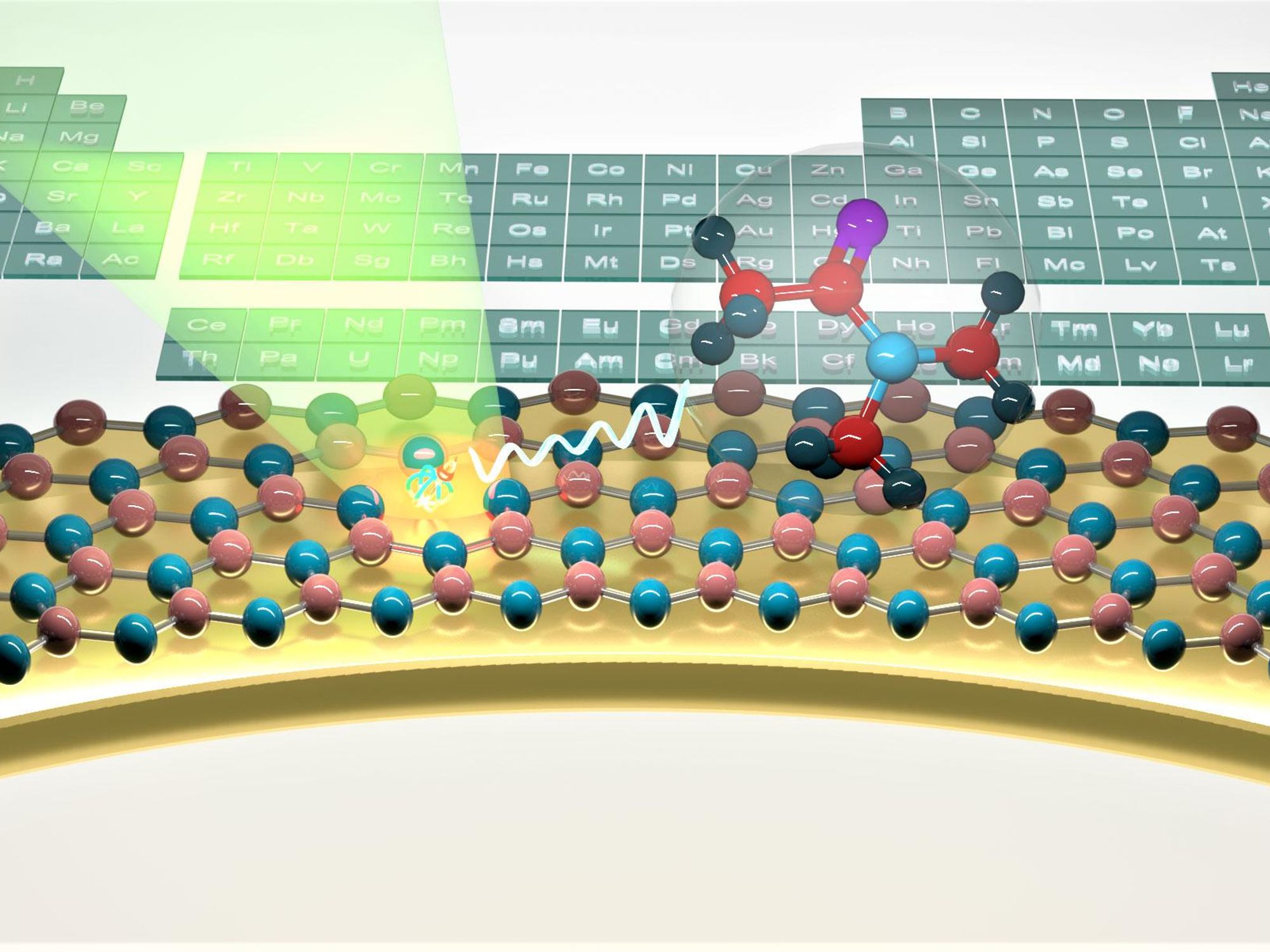
Quantum microscopy uses quantum sensors to map the magnetic, electrical, thermal, and other features of samples at microscopic scales. In the new study, researchers developed a prototype quantum microscope based on flakes of hexagonal boron nitride. This ceramic often finds use as an insulating material in atomically thin 2D electronics.
“One can … have millions of sensors on your fingertips. This is much harder to nearly impossible with any other system.”
—Alexander Healey, University of Melbourne
The prototype microscopy system places hexagonal boron nitride flakes 10 to 100 nanometers thick on top of samples. These samples possess defects wherein boron atoms are missing. When these negatively charged vacancies are illuminated with a green laser beam, they fluoresce with near-infrared light. Magnetic, electrical, thermal and other disturbances can alter this response, allowing these defects to help serve as sensors. Each hexagonal boron nitride flake is essentially an array of sensors.
In experiments, the scientists analyzed a flake of chromium telluride, a material that is magnetic just above room temperature. Magnetic materials are often divided into domains in which the magnetic poles all point in the same direction. The researchers were able to image the magnetic domains of the sample under ambient conditions, something that was previously believed impossible.
In addition, the scientists could map the thermal and magnetic features of the chromium telluride flake at the same time to see the links between temperature and magnetism in the sample. They could also map out charge currents and heating in a graphene device as it operated.
«Mapping temperature and magnetic properties at the same time in an operating spintronic device would be useful because we could see which parts of the device get hotter and how it locally affects the magnetic properties, which would greatly help in understanding the overall performance of the device,» says study co-lead author Alexander Healey, a physicist at the University of Melbourne.
A quantum microscope could also map the atomic structures of molecules, essentially «realizing atomic-scale MRI,» Healey says. «This would be extremely useful for biomedical research, because it may allow us to map the atomic structure of some biomolecules that currently evade standard techniques of structure determination.»
Hexagonal boron nitride could also find use in remote sensing applications, «mainly for measuring magnetic fields with high accuracy and precision, beyond what’s possible with existing technology,» Healey says. «There are many potential applications of these quantum magnetometers—for example detecting anomalies in the Earth’s magnetic field to detect hidden objects and resource exploration, mapping underground minerals such as iron. One may not need to drill massive hole, but just stick a fiber containing hexagonal boron nitride down a few hundred meters to get a signal.»
Hexagonal boron nitride is made of layers held together by weak electric forces known as van der Waals interactions, the same forces that often make adhesive tapes sticky. Researchers can peel films off so-called van der Waals materials that are essentially 2D in nature. This means the new quantum microscope could its sensors just a few atoms away from the samples it is probing, leading to improved resolution and sensitivity. In contrast, previous quantum microscopy relied on rigid 3D crystals such as diamond. These sensors could only come within a few dozen nanometers from samples at best, limiting how much thy could detect.
“This is a big advantage over SQUID quantum microscopy, for example, which will always require low temperatures, preventing operation in ambient conditions, let alone in liquids.”
—Alexander Healey, University of Melbourne
«The closer the sensor is to the sample, the easier it is for the sensor to detect very minute signals from the sample, and details on smaller length scales,» Healey says.
The scientists note that in the hexagonal boron nitride flakes they used, only a few of the defects came within atomic proximity of the sample. Instead, most of the defects were on average roughly 20 nanometers from the sample for the 40-nanometer-flake used in most of their experiments. As such, the new quantum microscope is not as sensitive as state-of-the-art diamond-based quantum microscopes, although it possessed comparable spatial resolution. (Specifically, the prototype achieved a spatial resolution of about 1 micron, a magnetic sensitivity of about 100 microTesla and a thermal sensitivity of about 5 Kelvin.)
In the future, the researchers seek to selectively create defects on in the atomic layers of the hexagonal boron nitride flakes closest to the samples, or to use thinner flakes. Such improvements could help lead their quantum microscope to realize a spatial resolution of 10 nanometers and a hundred-fold boost in sensitivity, they say.
In addition, the researchers note that hexagonal boron nitride quantum microscopy, like diamond-based quantum microscopy, can operate in a wide variety of conditions. These include from cryogenic to well above room temperatures, from vacuum to very high pressures, and in liquid settings.
«This is a big advantage over SQUID quantum microscopy, for example, which will always require low temperatures, preventing operation in ambient conditions, let alone in liquids,» Healey says.
Furthermore, it is relatively simple to prepare hexagonal boron nitride flakes. «One can exfoliate hexagonal boron nitride with Scotch tape and have millions of sensors on your fingertips,» Healey says. «This is much harder to nearly impossible with any other system.»
Moreover, hexagonal boron nitride is often already incorporated within nanotechnology—for instance, used to encapsulate more delicate materials, Healey says. As such, there should be little in the way of worries when it comes to how it might affect any properties of the samples getting analyzed, Healey says. «Using a high-power laser can, of course, be invasive, but we found that the power could be lowered to the point of negligible heating while maintaining our ability to sense,» he adds.
The scientists continue to look for materials that might prove even better for quantum microscopy than hexagonal boron nitride. «We expect this search for the ideal quantum sensor will be an important direction of future research,» Healey says.
The scientists detailed their findings this month in the journal Nature Physics.
Source: IEEE Spectrum Computing