
The most advanced manufacturers of computer processors are in the middle of the first big change in device architecture in a decade—the shift from finFETs to nanosheets. Another ten years should bring about another fundamental change, where nanosheet devices are stacked atop each other to form complementary FETs (CFETs), capable of cutting the size of some circuits in half. But the latter move is likely to be a heavy lift, say experts. An in-between transistor called the forksheet might keep circuits shrinking without quite as much work.
The idea for the forksheet came from exploring the limits of the nanosheet architecture, says Julien Ryckaert, the vice president for logic technologies at Imec. The nanosheet’s main feature is its horizontal stacks of silicon ribbons surrounded by its current-controlling gate. Although nanosheets only recently entered production, experts were already looking for their limits years ago. Imec was tasked with figuring out “at what point nanosheet will start tanking,” he says.
Ryckaert’s team found that one of the main limitations to shrinking nanosheet-based logic is keeping the separation between the two types of transistor that make up CMOS logic. The two types—NMOS and PMOS—must maintain a certain distance to limit capacitance that saps the devices’ performance and power consumption. “The forksheet is a way to break that limitation,” Ryckaert says.
Instead of individual nanosheet devices, the forksheet scheme builds them as pairs on either side of a dielectric wall. (No, it doesn’t really resemble a fork much.) The wall allows the devices to be placed closer together without causing a capacitance problem, says Naoto Horiguchi, the director of CMOS technology at Imec. Designers could use the extra space to shrink logic cells, or they could use the extra room to build transistors with wider sheets leading to better performance, he says.
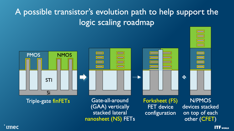
Leading-edge transistors are already transitioning from the fin field-effect transistor (FinFET) architecture to nanosheets. The ultimate goal is to stack two devices atop each other in a CFET configuration. The forksheet may be an intermediary step on the way.Imec
“CFET is probably the ultimate CMOS architecture,” says Horiguchi of the device that Imec expects to reach production readiness around 2032. But he adds that CFET “integration is very complex.” Forksheet reuses most of the nanosheet production steps, potentially making it an easier job, he says. Imec predicts it could be ready around 2028.
There are still many hurdles to leap over, however. “It’s more complex than initially thought,” Horiguchi says. From a manufacturing perspective, the dielectric wall is a bit of a headache. There are several types of dielectric used in advanced CMOS and several steps that involve etching it away. Making forksheets means etching those others without accidentally attacking the wall. And it’s still an open question which types of transistor should go on either side of the wall, Horiguchi says. The initial idea was to put PMOS on one side and NMOS on the other, but there may be advantages to putting the same type on both sides instead.
Source: IEEE Semiconductors