The most advanced processors today are no longer a single piece of silicon. Instead they are multiple “chiplets” bound together by advanced packaging techniques that do their best to make it seem as if everything really is one big chip. But many of these tricks are expensive and yield too many failed systems. Eliyan, a startup in Santa Clara, Calif., says it has technology that can make chiplets more affordable and reliable, by using less-advanced packaging.
Advanced packaging, often called 2.5D and 3D packaging, relies on the fact that signal-carrying interconnects can be made much more densely on relatively expensive silicon than on the cheaper organic substrate of a typical chip package. In two-dimensions, the less expensive option, that can mean placing chiplets within a hundred or so micrometers of each other on a silicon interposer, a relatively large slice semiconductor into which a dense set of interconnects have been constructed. Or the two chiplets can be linked by a small silicon bridge, set into the substrate.
Eliyan founder Ramin Farjadrad says there are problems with both schemes and that his startup’s NuLink technology can do just as well without the silicon. “The main problem with interposers is that they are size limited,” says Farjadrad. Because they are made using the same processes and equipment as microchips, it’s difficult to make them bigger than the biggest microchip—about 800 square millimeters. (That’s not counting Cerebras wafer-scale processor, of course.)
What’s more, linking chiplets to these silicon substrates, be they an interposer or a bridge, means building more densely-packed and therefore delicate connections on the face of the chiplet itself. These connections are typically small bumps of solder. Linking to an organic package uses bumps separated by more than 100 micrometers. But silicon bridges need what are called microbumps, which are placed as little as 30 micrometers apart. Microbumps are more prone to failure than ordinary bumps, says Farjadrad, and they make it difficult to test a chiplet before it’s placed on the substrate.
Eliyan’s solution, NuLink, is a proprietary technology that allows interconnects on organic substrates to match the data throughput of interposer-enabled 2.5D technologies. Such throughput is measured in bits per second per millimeter of the edge of an IC, and Eliyan’s recently designed version should reach at least 2 terabits/s/mm. That matches the maximum for the recently adopted Universal Chiplet Interconntect Express (UCIe) standard, and NuLink is backward compatible with it, says Farjadrad.
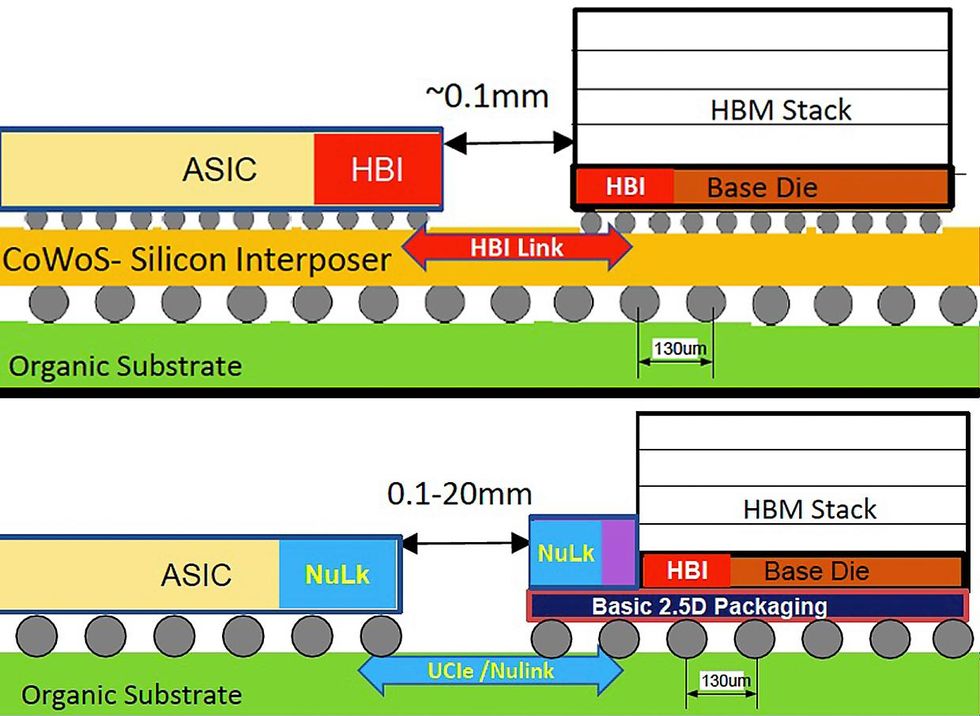
Compared to today’s methods [top], Eliyan’s NuLink [bottom] would let high-bandwidth memory sit farther away from processors using less expensive and more reliable physical links, while maintaining bandwidthEliyan
What’s the advantage then? Farjadrad has a long list. First, there is the simple advantage of being able to use a less expensive substrate and connecting to it with a more reliable interface to the chiplet. The second is the scheme’s low power consumption and low latency, the time it takes for the signal to leave one chiplet and arrive inside another. Other schemes for organic substrates can reach the terabit/s/mm mark, but they consume twice or more the energy to deliver each bit, have higher latency, or both.
“We’re not claiming to beat advanced packaging,” says Farjadrad. “But by providing 2-4Tb/s/mm bandwidth, we can address a large portion of the applications without a silicon interposer.”
Eliyan’s first target for its tech is linking high-bandwidth memory (HBM) to CPUs and GPUs. One of the biggest bottlenecks to pushing machine learning further is keeping the processor fed with data as fast as possible. That means putting memory chips as close as possible to the processor and using high-bandwidth links. Advanced processors such as Intel’s Ponte Vecchio are literally surrounded by HBM attached to the processor with a silicon interposer or using a silicon bridge. By adding NuLink to both the HBM and the processor, companies could get the same result without the silicon. What’s more, because NuLink works over a distance of up to 20 millimeters, designers could stagger the HBM, making room for double the amount of memory, which according to Eliyan could triple a GPU’s performance.
The hitch is that it’s quite a big ask for a startup to tell memory giants that they should add proprietary circuitry to their silicon. So instead, Eliyan has designed an interposer of its own. The HBM joins Eliyan’s own NuLink chiplet on the interposer and the combination is attached to the organic substrate where it links to the processor. Eliyan’s first silicon, built using TSMC’s 5-nanometer process, should arrive in early 2023.
Source: IEEE Semiconductors