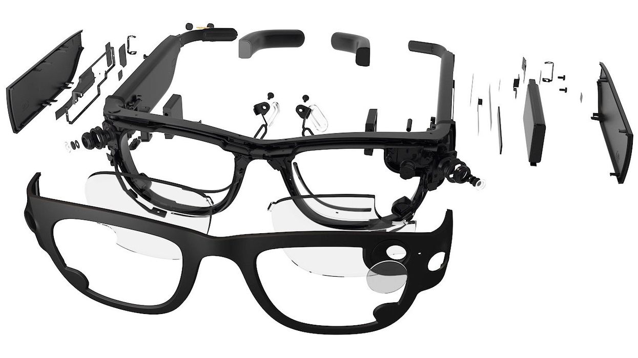
There are many constraints on the design of augmented reality systems. Not the least of which is that “you have to look presentable when you’re walking around,” Meta research scientist Tony Wu told engineers Tuesday at the IEEE International Solid State Circuits Conference (ISSCC). “You can’t have a shoebox on your face all the time.”
An AR system also must be lightweight and can’t throw off a lot of heat. And it needs to be miserly with power because nobody wants to have to recharge wearable electronics every couple of hours. Then again, if you’ve got a flaming hot shoebox on your face, you might be grateful for a short battery life.
The 3D chip could track two hands simultaneously using 40 percent less energy than a single-die could do with only one hand. What’s more, it did so 40 percent faster.
Wu is part of the Meta team working on the silicon smarts to make an AR system, called Aria, that’s the as little like a hot shoebox as they can make it. A big part of the solution, Wu told engineers, is 3D chip integration technology. At ISSCC, Meta detailed how the company’s prototype AR processor uses 3D to do more in the same area and with the same amount or less energy.
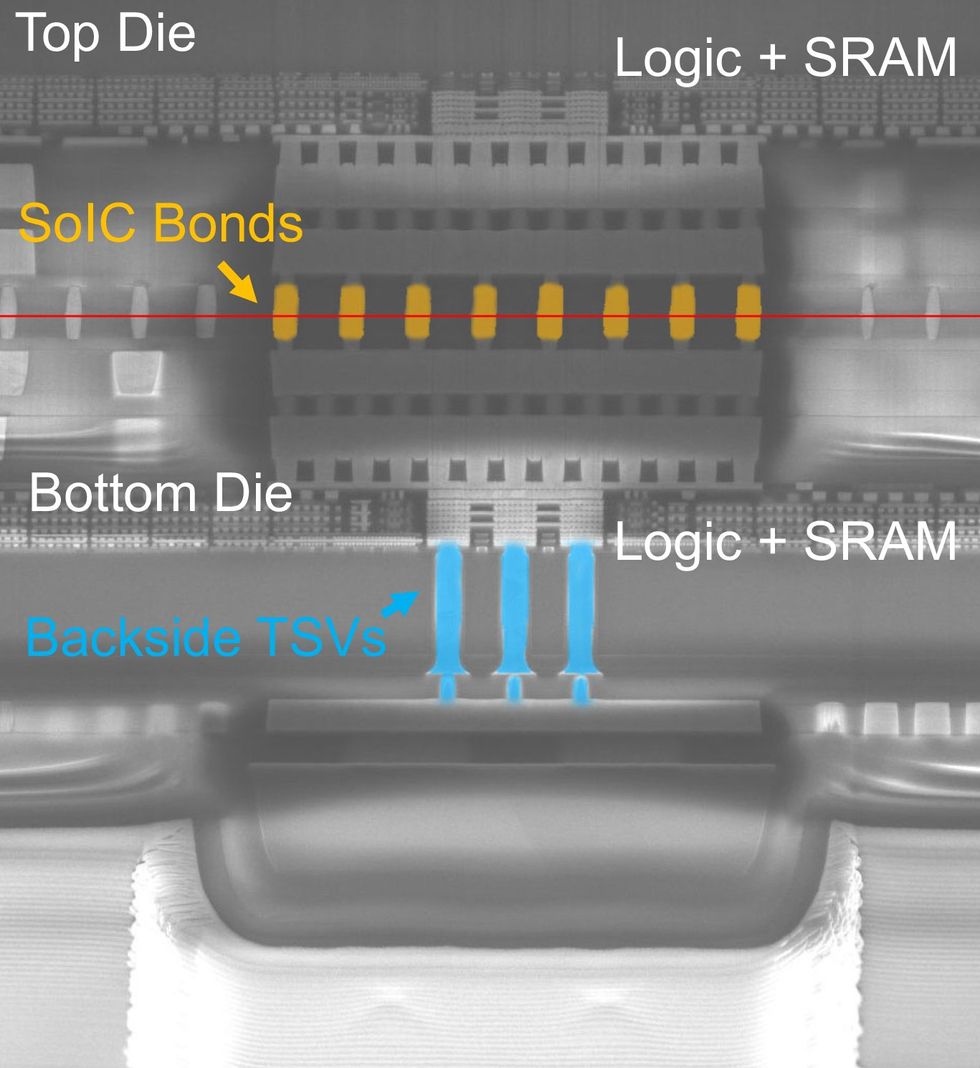
Meta’s prototype chip has both logic and memory on each silicon die. They’re bonded face-to-face and through-silicon vias (TSVs) carry data and power to both.Meta
The prototype chip is two ICs of equal size—4.1 x 3.7 millimeters. They’re bonded together in a process called face-to-face wafer-to-wafer hybrid bonding. As the name implies, it involves flipping two fully processed wafers so they’re facing each other and bonding them, so their interconnects link together directly. (The “hybrid bonding” part means it’s a direct copper-to-copper connection. No solder needed.)
The TSMC technology used for this meant the two pieces of silicon could form a vertical connection roughly every 2 micrometers. The prototype didn’t fully make use of this density: It required around 33,000 signal connections between the two pieces of silicon and 6 million power connections. The bottom die uses through-silicon vias—vertical connections bored down through the silicon—to get signals out of the chip and power in.
3D stacking meant the team could increase the chip’s computing power—letting it handle bigger tasks—without adding to its size. The chip’s machine learning unit has four compute cores on the bottom die and 1 megabyte of local memory, but the top die adds another 3 MB, accessible through 27,000 vertical data channels at the same speed and energy—0.15 picojoules/byte— as if they were one big piece of silicon.
The team tested the chip on a machine learning task critical for augmented reality, hand tracking. The 3D chip was able to track two hands simultaneously using 40 percent less energy than a single-die could do with only one hand. What’s more, it did so 40 percent faster.
In addition to machine learning, the chip can do image processing tasks. 3D made a big difference here, again. While the 2D version was limited to compressed images, the 3D chip can do full HD using the same amount of energy.
Source: IEEE Semiconductors