In 2016, the Japanese government announced a plan for the emergence of a new kind of society. Human civilization, the proposal explained, had begun with hunter-gatherers, passed through the agrarian and industrial stages, and was fast approaching the end of the information age. As then Prime Minister Shinzo Abe put it, “We are now witnessing the opening of the fifth chapter.”
This chapter, called
Society 5.0, would see made-on-demand goods and robot caretakers, taxis, and tractors. Many of the innovations that will enable it, like artificial intelligence, might be obvious. But there is one key technology that is easy to overlook: lasers.
The lasers of Society 5.0 will need to meet several criteria. They must be small enough to fit inside everyday devices. They must be low-cost so that the average metalworker or car buyer can afford them—which means they must also be simple to manufacture and use energy efficiently. And because this dawning era will be about mass customization (rather than mass production), they must be highly controllable and adaptive.
Semiconductor lasers would seem the perfect candidates, except for one fatal flaw: They are much too dim. Laser brightness—defined as optical power per unit area per unit of solid angle—is a measure of how intensely light can be focused as it exits the laser and how narrowly it diverges as it moves away. The threshold for materials work—cutting, welding, drilling—is on the order of 1 gigawatt per square centimeter per steradian (GW/cm2/sr). However, the brightness of even the brightest commercial semiconductor lasers falls far below that.
Brightness is also important for light detection and ranging (lidar) systems in autonomous robots and vehicles. These systems don’t require metal-melting power, but to make precise measurements from long distances or at high speeds, they do require tightly focused beams. Today’s top-line lidar systems employ more than 100 semiconductor lasers whose inherently divergent beams are collimated using a complicated setup of lenses installed by hand. This complexity drives up cost, putting lidar-navigated cars out of reach for most consumers.
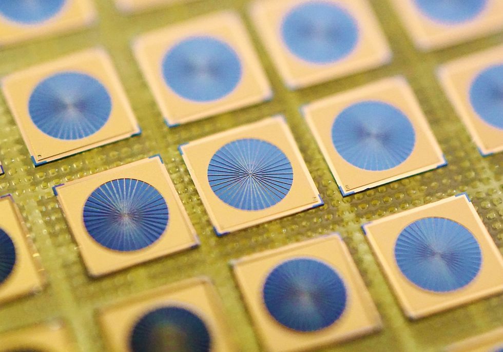
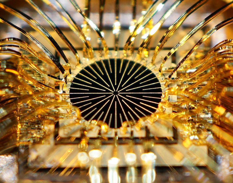
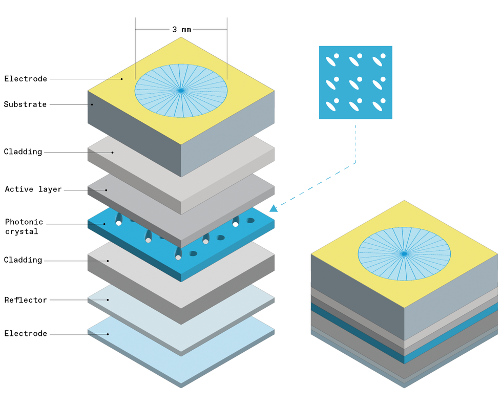
Multiple 3-millimeter-wide photonic-crystal semiconductor lasers are built on a semiconductor wafer. Susumu Noda
Of course, other types of lasers can produce ultrabright beams. Carbon dioxide and
fiber lasers, for instance, dominate the market for industrial applications. But compared to speck-size semiconductor lasers, they are enormous. A high-power CO2 laser can be as large as a refrigerator. They are also more expensive, less energy efficient, and harder to control.
Over the past couple of decades, our team at Kyoto University has been developing a new type of semiconductor laser that blows through the brightness ceiling of its conventional cousins. We call it the
photonic-crystal surface-emitting laser, or PCSEL (pronounced “pick-cell”). Most recently, we fabricated a PCSEL that can be as bright as gas and fiber lasers—bright enough to quickly slice through steel—and proposed a design for one that is 10 to 100 times as bright. Such devices could revolutionize the manufacturing and automotive industries. If we, our collaborating companies, and research groups around the world—such as at National Yang Ming Chiao Tung University, in Hsinchu, Taiwan; the University of Texas at Arlington; and the University of Glasgow—can push PCSEL brightness further still, it would even open the door to exotic applications like inertial-confinement nuclear fusion and light propulsion for spaceflight.
Hole-y Grail
The magic of PCSELs arises from their unique construction. Like any semiconductor laser, a PCSEL consists of a thin layer of light-generating material, known as the active layer, sandwiched between cladding layers. In fact, for the sake of orientation, it’s helpful to picture the device as a literal sandwich—let’s say a slice of ham between two pieces of bread.
Now imagine lifting the sandwich to your mouth, as if you are about to take a bite. If your sandwich were a conventional semiconductor laser, its beam would radiate from the far edge, away from you. This beam is created by passing a current through a stripe in the active “ham” layer. The excited ham atoms spontaneously release photons, which stimulate the release of identical photons, amplifying the light. Mirrors on each end of the stripe then repeatedly reflect these waves; because of interference and loss, only certain frequencies and spatial patterns—or modes—are sustained. When the gain of a mode exceeds losses, the light emerges in a coherent beam, and the laser is said to oscillate in that mode.
The problem with this standard stripe approach is that it is very difficult to increase output power without sacrificing beam quality. The power of a semiconductor laser is limited by its emission area because extremely concentrated light can cause catastrophic damage to the semiconductor. You can deliver more power by widening the stripe, which is the strategy used for so-called broad-area lasers. But a wider stripe also gives room for the oscillating light to take zigzag sideways paths, forming what are called higher-order lateral modes.
More Modes, More Problems
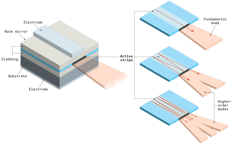
You can visualize the intesity pattern of a lateral mode by imagining that you’ve placed a screen in the cross section of the output beam. Light bouncing back and forth perfectly along the length of the stripe forms the fundamental (zero-order) mode, which has a single peak of intensity in the center of the beam. The first-order mode, from light reflecting at an angle to the edge of the sandwich, has two peaks to the right and left; the second-order mode, from a smaller angle, has a row of three peaks, and so on. For each higher-order mode, the laser effectively operates as a combination of smaller emitters whose narrower apertures cause the beam to diverge rapidly. The resulting mixture of lateral modes therefore makes the laser light spotty and diffuse.
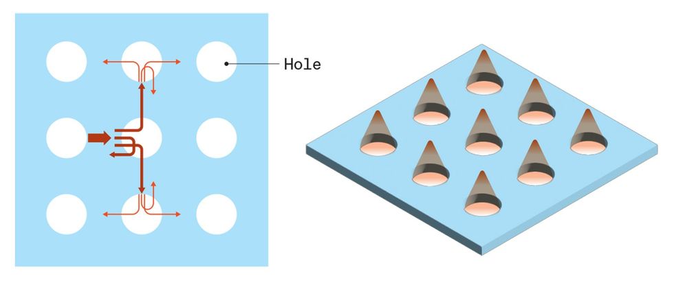
Those troublesome modes are why the brightness of conventional semiconductor lasers maxes out around 100 MW/cm2/sr. PCSELs deal with unwanted modes by adding another layer inside the sandwich: the “Swiss cheese” layer. This special extra layer is a semiconductor sheet stamped with a two-dimensional array of nanoscale holes. By tuning the spacing and shape of the holes, we can control the propagation of light inside the laser so that it oscillates in only the fundamental mode, even when the emission area is expanded. The result is a beam that can be both powerful and narrow—that is, bright.
Because of their internal physics, PCSELs operate in a completely different way from edge-emitting lasers. Instead of pointing away from you, for instance, the beam from your PCSEL sandwich would now radiate upward, through the top slice of bread. To explain this unusual emission, and why PCSELs can be orders of magnitude brighter than other semiconductor lasers, we must first describe the material properties of the Swiss cheese—in actuality, a fascinating structure called a photonic crystal.
How Photonic Crystals Work
Photonic crystals control the flow of light in a way that’s similar to how semiconductors control the flow of electrons. Instead of atoms, however, the lattice of a photonic crystal is sculpted out of larger entities—such as holes, cubes, or columns—arranged such that the refractive index changes periodically on the scale of a wavelength of light. Although the quest to artificially construct these marvelous materials began less than 40 years ago, scientists have since learned that they already exist in nature. Opals, peacock feathers, and some butterfly wings, for example, all owe their brilliant iridescence to the intricate play of light within naturally engineered photonic crystals.
Understanding how light moves in a photonic crystal is fundamental to PCSEL design. We can predict this behavior by studying the crystal’s photonic band structure, which is analogous to the electronic band structure of a semiconductor. One way to do that is to plot the relationship between frequency and wavenumber—the number of wave cycles that fit within one unit cell of the crystal’s lattice.
How Light Moves in a Photonic Crystal
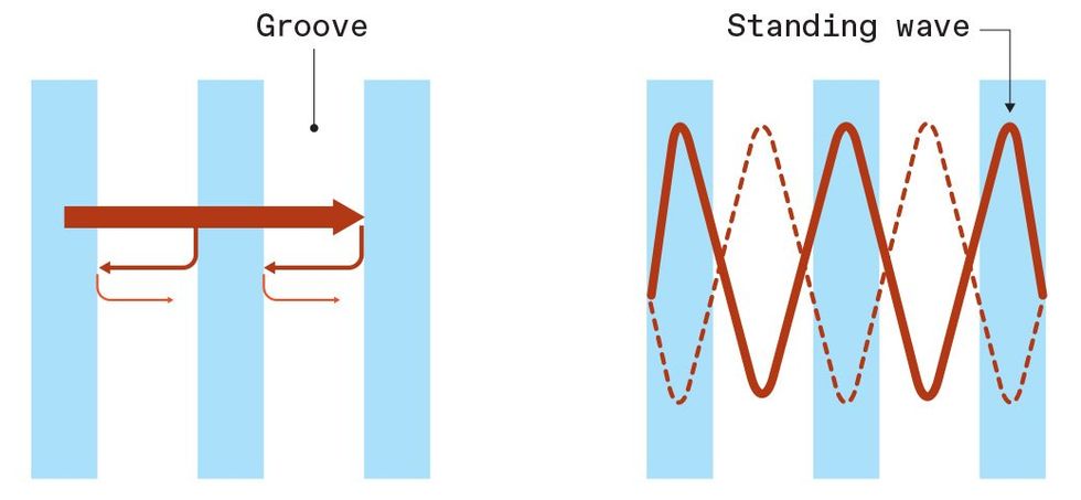
Consider, for example, a simple one-dimensional photonic crystal formed by alternating ribbons of glass and air. Light entering the crystal will refract through and partially reflect off each interface, producing overlapping beams that reinforce or weaken one another according to the light’s wavelength and direction. Most waves will travel through the material. But at certain points, called singularity points, the reflections combine perfectly with the incident wave to form a standing wave, which does not propagate. In this case, a singularity occurs when a wave undergoes exactly half a cycle from one air ribbon to the next. There are other singularities wherever a unit cell is an integer multiple of half the wavelength.
One of us (Susumu Noda) began experimenting with lasers containing photonic crystal-like structures before these materials even had a name. In the mid 1980s, while at Mitsubishi Electric Corporation, he studied a semiconductor laser called a distributed feedback (DFB) laser. A DFB laser is a basic stripe laser with an extra internal layer containing regularly spaced grooves filled with matter of a slightly different refractive index. This periodic structure behaves somewhat like the 1D photonic crystal described above: It repeatedly reflects light at a single wavelength, as determined by the groove spacing, such that a standing wave emerges. Consequently, the laser oscillates at only that wavelength, which is critical for long-haul fiber-optic transmission and high-sensitivity optical sensing.
Steel Slicer
As the Mitsubishi team demonstrated, a DFB laser can be enticed to perform other tricks. For instance, when the team set the groove spacing equal to the lasing wavelength in the device, some of the oscillating light diffracted upward, causing the laser to shine not only from the tiny front edge of its active stripe but also from the stripe’s top. However, this surface beam fanned wildly due to the narrow width of the stripe, which also made it difficult to increase the output power.
To Noda’s disappointment, his team’s attempts to widen the stripe—and therefore increase brightness—without causing other headaches were unsuccessful. Nevertheless, those early failures planted an intriguing idea: What if laser light could be controlled in two dimensions instead of one?
Boosting Brightness
Later, at Kyoto University, Noda led research into 2D and 3D photonic crystals just as the field was coming into being. In 1998, his team built the first PCSEL, and we have since honed the design for various functionalities, including high brightness.
In a basic PCSEL, the photonic-crystal layer is a 2D square lattice: Each unit cell is a square delineated by four holes. Although the band structure of a 2D photonic crystal is more complicated than that of a 1D crystal, it likewise reveals singularities where we expect standing waves to form. For our devices, we have made use of the singularity that occurs when the distance between neighboring holes is one wavelength. A gallium arsenide laser operating at 940 nanometers, for example, has an internal wavelength of around 280 nm (considering refractive index and temperature). So the holes in a basic gallium arsenide PCSEL would be set about 280 nm apart.
The operating principle is this: When waves of that length are generated in the active layer, the holes in the neighboring photonic-crystal layer act like tiny mirrors, bending the light both backward and sideways. The combined effect of multiple such diffractions creates a 2D standing wave, which is then amplified by the active layer. Some of this oscillating light also diffracts upward and downward and leaks out the laser’s top, producing a surface beam of a single wavelength.
A key reason this design works is the large refractive index contrast between the semiconductor and the air inside the holes. As Noda discovered while creating the first device, PCSELs with low refractive index contrasts, like those of DFB lasers, do not oscillate coherently. Also unlike a DFB laser, a PCSEL’s surface emission area is broad and usually round. It can therefore produce a higher quality beam with much lower divergence.
Bigger and Brighter
As PCSEL size grows to accommodate more optical power, more lateral modes begin to oscillate. Here’s how those modes are eliminated in each device generation.
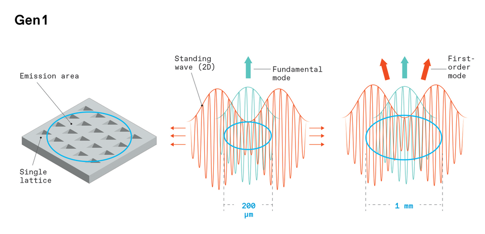
Higher-order lateral modes form when a standing wave has multiple average peaks of intensity. When the emission area of the PCSEL is relatively small, the peaks sit near its edge. Consequently, most of the light leaks out of the sides, and so the higher-order modes do not oscillate.
The double lattice causes light diffracting through the crystal to interfere destructively. These cancellations weaken and spread the intensity peaks of the standing waves, causing the higher-order modes to leak heavily again. However, this method alone does not sufficiently suppress those modes in larger devices.
Adjustments to the holes and the bottom reflector induce light exiting the laser to lose some of its energy through interference with the standing waves. Because higher-order modes lose more light, they can be selectively cut off.
In 2014, our group reported that a PCSEL with a square lattice of triangular holes and an emission area of 200 by 200 μm could operate continuously at around 1 watt while maintaining a spotlike beam that diverged only about 2 degrees. Compared with conventional semiconductor lasers, whose beams typically diverge more than 30 degrees, this performance was remarkable. The next step was to boost optical power, for which we needed a larger device. But here we hit a snag.
According to our theoretical models, PCSELs using the single-lattice design could not grow larger than about 200 μm without inviting pesky higher-order lateral modes. In a PCSEL, multiple modes form when the intensity of a standing wave can be distributed in multiple ways due to the interference pattern created by repeated diffractions. In the fundamental (read: desirable) mode, the intensity distribution resembles Mount Fuji, with most of the oscillating light concentrated in the center of the lattice. Each higher-order mode, meanwhile, has two, three, four, or more Mount Fujis. So when the laser’s emission area is relatively small, the intensity peaks of the higher-order modes sit near the lattice’s periphery. Most of their light therefore leaks out of the sides of the device, preventing these modes from oscillating and contributing to the laser beam. But as with conventional lasers, enlarging the emission area makes space for more modes to oscillate.
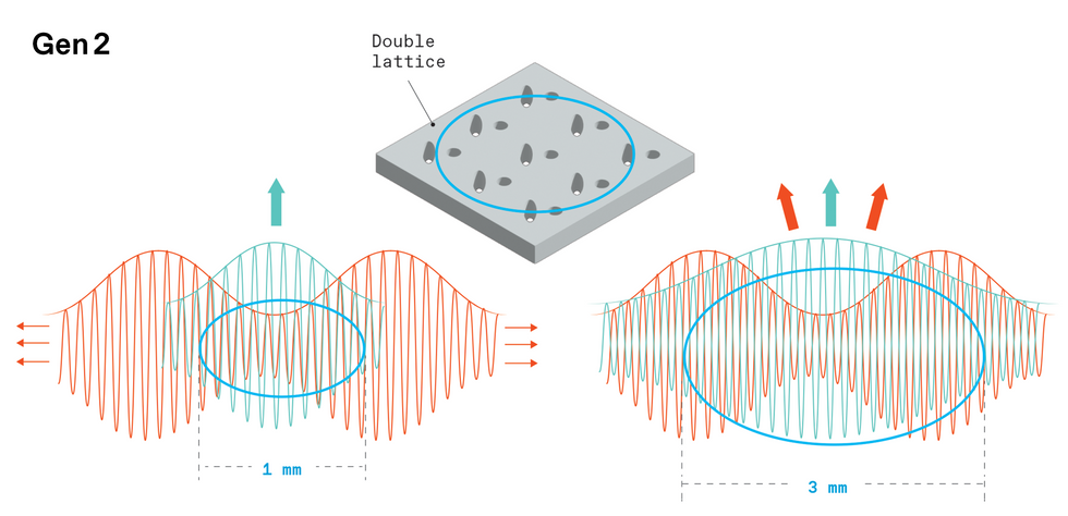
To solve that problem, we added another set of holes to the photonic-crystal layer, creating a double lattice. In our most successful version, a square lattice of circular holes is shifted a quarter wavelength from a second square lattice of elliptical holes. As a result, some of the diffracting light inside the crystal interferes destructively. These cancellations cause the intensity peaks of the lateral modes to weaken and spread. So when we expand the laser’s emission area, light from the higher-order modes still leaks heavily and does not oscillate.
Using that approach, we fabricated a PCSEL with a round emission area 1 millimeter in diameter and showed it could produce a 10-W beam under continuous operation. Diverging just one-tenth of a degree, the beam was even slenderer and more collimated than its 200-μm predecessor and more than three times as bright as is possible with a conventional semiconductor laser. Our device also had the advantage of oscillating in a single mode, of course, which conventional lasers of comparable size cannot do.
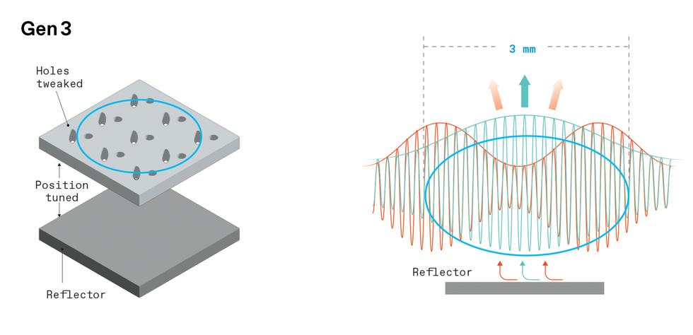
Pushing PCSEL brightness higher required further innovation. At larger diameters, the double-lattice approach alone does not sufficiently suppress higher-order modes, and so they oscillate yet again. We had observed, however, that these modes depart the laser slightly askew, which drew our attention to the backside reflector. (Picture a sheet of tinfoil lining the bottom of your ham and Swiss sandwich.)
This 50-watt PCSEL is bright enough to slice through steel.
Susumu Noda
In previous device generations, this reflector had served simply to bounce downward-diffracted light up and out from the laser’s emitting surface. By adjusting its position (as well as the spacing and shape of the photonic-crystal holes), we found we could control the reflections so that they interfere in a useful way with the 2D standing waves oscillating within the photonic-crystal layer. This interference, or coupling, essentially induces the departing waves to lose some of their energy. The more askew a departing wave, the more light is lost. And poof! No more higher-order modes.
That is how, in 2023, we developed a PCSEL whose brightness of 1 GW/cm2/sr rivals that of gas and fiber lasers. With a 3-mm emission diameter, it could lase continuously at up to 50 W while sustaining a beam that diverged a minuscule one-twentieth of a degree. We even used it to cut through steel. As the bright, beautiful beam carved a disc out of a metal plate 100 μm thick, our entire lab huddled around, watching in amazement.
More Powerful PCSELs
As impressive as the steel-slicing demonstration was, PCSELs must be even more powerful to compete in the industrial marketplace. Manufacturing automobile parts, for instance, requires optical powers on the order of kilowatts.
It should be fairly straightforward to build a PCSEL that can handle that kind of power—either by assembling an array of nine 3-mm PCSELs or by expanding the emission area of our current device to 1 cm. At that size, higher-order modes would once again emerge, reducing the beam quality. But because they would still be as bright as high-power gas and fiber lasers, such kilowatt-class PCSELs could begin to usurp their bulkier competitors.
To be truly game-changing, 1-cm PCSELs would need to level up by suppressing those higher-order modes. We have already devised a way to do that by fine-tuning the photonic-crystal structure and the position of the reflector. Although we have not yet tested this new recipe in the lab, our theoretical models suggest that it could raise PCSEL brightness as high as 10 to 100 GW/cm2/sr. Just imagine the variety of unique and intricate products that could be made when such concentrated light can be wielded from a tiny package.
Especially for those high-power applications, we’ll need to improve the laser’s energy efficiency and thermal management. Even without any optimization, the “wall plug” efficiency of PCSELs is already at 30 to 40 percent, exceeding most carbon-dioxide and fiber lasers. What’s more, we’ve found a path we think could lead to 60 percent efficiency. And as for thermal management, the water-cooling technology we’re using in the lab today should be sufficient for a 1,000-W, 1-cm PCSEL.
High-brightness PCSELs could also be used to make smaller and more affordable sensor systems for self-driving cars and robots. Recently, we built a lidar system using a 500-μm PCSEL. Under pulsed operation, we ran it at about 20 W and got a terrifically bright beam. Even at 30 meters, the spot size was only 5 cm. Such high resolution is unheard of for a compact lidar system without external lenses. We then mounted our prototypes—which are roughly the size of a webcam—on robotic carts and programmed them to follow us and one another around the engineering building.
In a separate line of work, we have shown that PCSELs can emit multiple beams that can be controlled electronically to point in different directions. This on-chip beam steering is achieved by varying the position and size of the holes in the photonic-crystal layer. Ultimately, it could replace mechanical beam steering in lidar systems. If light detectors were also integrated on the same chip, these all-electronic navigation systems would be seriously miniature and low-cost.
Although it will be challenging, we eventually hope to make 3-cm lasers with output powers exceeding 10 kilowatts and beams shining up to 1,000 GW/cm2/sr—brighter than any laser that exists today. At such extreme brightness, PCSELs could replace the huge, electricity-hungry CO2 lasers used to generate plasma pulses for extreme ultraviolet lithography machines, making chip manufacturing much more efficient. They could similarly advance efforts to realize nuclear fusion, a process that involves firing trillions of watts of laser power at a pea-size fuel capsule. Exceptionally bright lasers also raise the possibility of light propulsion for spaceflight. Instead of taking thousands of years to reach faraway stars, a probe boosted by light could make the journey in only a few decades.
It may be a cliché, but we cannot think of a more apt prediction for the next chapter of human ingenuity: The future, as they say, is bright.
Source: IEEE Semiconductors