No doping or nanostructuring is required for new bottom-up method to grow graphene with a perfect band gap

For all of graphene’s amazing electronic capabilities, it has not made much of an impact as a replacement for silicon in digital logic applications. This shortcoming is largely due to its lack of an inherent band gap that’s needed in computing applications to start and stop the flow of electrons.
While methods for engineering a band gap into graphene have been around for years, these approaches have been recognized as imperfect solutions. They have added critical costs and complications to using the material and compromised the attractive electronic properties that made graphene a desirable replacement for silicon in the first place.
Now researchers in Spain have devised an inexpensive way to grow graphene with the same band gap that exists in silicon (1 eV), and in so doing, may have reopened graphene’s potential as an alternative to silicon for digital logic.
In research described in the journal
Science
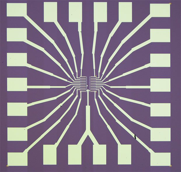
, a team from throughout Spain and led by the Catalan Institute of Nanoscience and Nanotechnology (ICN2) has employed bottom-up manufacturing techniques to assemble nanopororus graphene in such a way that the pores have the size, density, and morphology to create a perfect band gap for digital electronics. The researchers then made a field-effect transistor (FET) device using this material.
“What we show in our work is that it is possible to fabricate a graphene ‘like’ material, but with a gap that is very close to the one of silicon, said Aitor Mugarza, a research professor and group leader at ICN2. “In addition, by simply modifying the width of the graphene strips between the pores (the number of carbon atoms), this band gap can be controlled. The fabrication method is relatively simple and can be extended to wafer-scale growth.”
Currently, the main methods to induce a band gap into graphene involve chemical doping or adding pores, or reducing it into nanoribbons—processes known as nanostructuring.
Nanostructuring graphene with current top-down fabrication methods—either by cutting down carbon nanotubes or slicing strips out of graphene—struggles to reach the scale of a few nanometers with atomic precision. This level of precision is required to induce a sizable, homogenous band gap that would enable room temperature applications, according to Mugarza.
“The bottom-up synthesis approach allows the fabrication of one-dimensional graphene nanoribbons and, as we show in this work, nanoporous structures with atomic precision and with lateral dimensions in the order of 1 nm,” said Mugarza. “This is the crucial ingredient to obtain a sizeable and homogeneous gap.”
Mugarza explains that until now, nobody has fully exploited these bottom-up techniques for graphene because of the difficulty in fabricating devices using these tiny structures. But because of the larger dimensions of the nanoporous graphene produced by the Spanish researchers, it has become possible to fabricate devices with high yield using standard lithographic techniques.
The semiconducting character of the material that Spanish researchers have developed is only indirectly related to the pores, according to Mugarza. The semiconducting gap is, in fact, related to the finite lateral size of the graphene sections that are between the pores. The individual nanoribbons are already semiconductors before coupling with each other to form pores.
While the size of the pores does not directly affect the band gap, the pore uniformity is correlated with uniformity in the gap value, but not to its absolute value, according to Mugarza. “In other words, the size of the graphene sections between the pores will define the absolute value of the gap, and variations on this size will induce inhomogeneities in the gap value,” he added.
At the scale of this work, a one-atom variation in the lateral dimensions of the sections between pores translates into large variations in the gap, so homogeneity is critical. “The structure of our nanoporous material is atomically homogeneous, and thus shows minimal gap inhomogeneities,” said Mugarza.
In the video below, you can see a computer simulation of the atomic scale precision involved in this work.
Mugarza concedes that work will need to be performed that is typical in working with graphene-based devices and semiconductors, such as contact engineering and using efficient dielectrics materials.
As for possible applications, the long road will be in pursuing those areas in which the material only acts as a semiconductor, such as in transparent semiconductors, electronic and opto-electronic devices, actuators and sensors. But Mugarza believes the main potential for this graphene will be in those areas that also exploit its selective permeability for additional functionality. In these areas, the most straightforward relevant applications are in gas sensing and filtering, along with water purification and desalination.
Source: IEEE Semiconductors